China CXMT Testing Production Line for Next-Gen Bonded DRAM, Closing Tech Gap With Korea “Far Faster Than Expected”
According to Korea’s Hankgyung, China’s largest memory company, CXMT, which is preparing to IPO in the coming weeks, is currently testing a pilot production line for bonded DRAM in Hefei (the heart of China’s semiconductor industry), aiming to achieve high-performance DRAM without using advanced EUV lithography, which is currently monopolized by Dutch ASML and faces unprecedented export controls (although according to Reuters, China has already built a prototype EUV machine).
Bonded DRAM is a technology in which the memory cell array and the peripheral circuitry are fabricated on separate wafers and then bonded together, as explained here. This approach enables the production of ultra-high-density DRAM using only deep ultraviolet (DUV) lithography with multi-patterning, eliminating the need for EUV tools.
Samsung Electronics is also developing its own bonded DRAM under the “B1b” project, while SK Hynix is pursuing a similar technology. However, Korean media warn that there are assessments suggesting CXMT may currently hold an edge over its Korean rivals in both the technology itself and the speed of development.
According to the Korean outlet, Chinese memory chipmakers CXMT (DRAM) and YMTC (NAND) – which just two years ago were nothing more than firms struggling to manufacture low-end chips and suffering trillions of won in losses annually – have recently undergone a dramatic transformation and have “closed the technology gap with Samsung Electronics and SK Hynix far faster than expected”, from roughly a 5-year lag down to about 3 years, despite US export controls blocking access to advanced EUV lithography equipment.
Here are the key details :
CXMT’s secret R&D push: At its Hefei facility, CXMT has secretly begun building an R&D line for next-generation “bonded DRAM,” aiming to commercialize it before Korean rivals. This project aims to develop and produce next-generation memory semiconductors known as “bonding DRAM.” These are considered “memory semiconductor game changers” because they can maximize performance and capacity. The company reportedly has recruited top-tier engineers with the explicit goal of beating Korea to market.
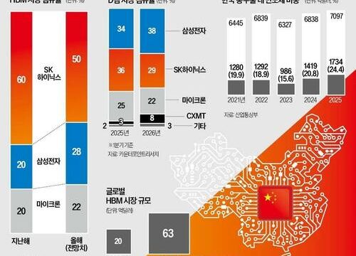
Rapid market gains: As recently as 2024, Chinese firms were seen as low-end, loss-making commodity suppliers. By Q1 2026, CXMT’s share of the global DRAM market reportedly jumped to 8%, and it’s said to be under consideration as a new DRAM supplier for Apple.
HBM ambitions: CXMT is pushing into high-bandwidth memory (HBM), converting about 20% of production lines toward HBM3/HBM3E development, working around the lack of EUV tools by using advanced multi-patterning with older DUV equipment.
NAND patents — China ahead: YMTC’s proprietary “Xtacking” wafer-bonding technology gave it an early lead in hybrid bonding patents — the article cites YMTC holding 119 core patents versus Samsung’s 83 and SK Hynix’s 11 (as of 2023) — to the point that Samsung reportedly licensed patents from YMTC for its next-gen NAND roadmap.
Next-gen tech race: Beyond HBM, China is pursuing “post-HBM” CXL (Compute Express Link) memory, with CXMT working with domestic fabless firm Montage Technology on controllers, leveraging its server DDR5 experience.
IPO push: Both CXMT and YMTC are moving toward public listings (CXMT possibly on the Shanghai exchange as soon as this month) to fund expansion beyond government subsidies.
Expert warnings: Seoul National University professor Hwang Chul-sung called Chinese semiconductors “the biggest future threat to Korea.” Another professor warned that once Chinese AI chipmakers like Huawei begin adopting domestic memory for real-world use, yield and reliability could improve faster than expected. A POSTECH professor argued Korea must lock in an unmatched technology lead in next-gen memory and packaging before the “golden time” created by U.S. sanctions runs out.
Also noted: Huawei’s May-unveiled “Tau’s Law” concept, which reportedly focuses on cutting data transfer time (rather than transistor miniaturization) to boost overall AI chip system performance — seen as a potentially disruptive alternative approach.
NAND flash and the hybrid bonding patent gap
The article frames this as the area where warning signs are already flashing red. Samsung and SK Hynix currently lead volume production in the 200-to-300+ layer NAND range, which underpins high-value products like enterprise SSDs. But pushing past 400 layers runs into physical limits, making “wafer-to-wafer (W2W) hybrid bonding” a must-have process — a technique that fuses two wafers directly, connecting circuits vertically without conductive bumps between chips.
China’s YMTC got there first. Its proprietary “Xtacking” architecture, the world’s first of its kind to reach commercialization, has scaled from 160-layer to the newest 270-layer NAND in mass production. On core patents, YMTC reportedly holds 119 versus Samsung’s 83 and SK Hynix’s 11 (2023 figures) — enough of a lead that Samsung, the NAND market leader, reportedly had to sign a patent licensing deal with YMTC to develop its next-generation “V10” triple-stack NAND (430+ layers).
The CXL / “post-HBM” race
Beyond memory’s current HBM cycle, the article describes China moving fast on CXL (Compute Express Link) DRAM, described as the “post-HBM” technology. CXMT is said to be leveraging its experience mass-producing server DDR5 to formally launch into CXL 3.0 development, and is partnering with domestic fabless chip designer Montage Technology to secure the controller technology that’s central to CXL products.
This sits alongside CXMT’s other next-gen bet: “bonded DRAM,” which separates the memory-cell layer and the peripheral control layer onto two different wafers before joining them – a way to boost density and performance without needing EUV lithography (which U.S. export controls block China from importing).
CXMT is reportedly piloting this at a Hefei line using older deep-ultraviolet (DUV) tools plus multi-patterning instead. Samsung (via its “B1b” project) and SK Hynix are working on their own bonded-DRAM equivalents, but the article notes some assessments actually rate CXMT ahead of the Korean firms on speed and technical maturity here.
A POSTECH professor is quoted arguing Korea’s current supply-chain lead owes a lot to U.S. sanctions on China, and that Korean chipmakers need to lock in an irreplaceable technology edge in next-gen memory and packaging before that sanctions-driven “golden window” closes.
Tyler Durden
Sun, 07/05/2026 – 21:42